10 Best Tips for Effective PCB Printing Techniques and Processes
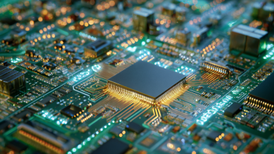
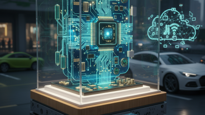
In the rapidly evolving field of electronics, the significance of "pcb printing" cannot be overstated. With the global PCB market projected to reach $96.5 billion by 2024, effective printing techniques are pivotal for manufacturers aiming to stay competitive. According to a recent industry report by IPC, approximately 70% of defects in PCB production are attributed to issues related to printing processes. As such, enhancing these methods has become critical for fostering product quality and reliability.
Expert in PCB design and manufacturing, Dr. Emily Thompson emphasizes the importance of precision in this domain: "The success of any electronic device hinges on the effectiveness of its PCB. Optimizing printing techniques is not just an option; it's a necessity." This statement highlights the role of advanced pcb printing techniques in mitigating defects and ensuring that manufacturers meet the stringent quality requirements of modern electronics. By implementing efficient processes, companies can significantly reduce waste and increase overall productivity. Exploring the best practices in pcb printing can ultimately lead to groundbreaking advancements in electronic design and functionality.

Understanding PCB Printing: Key Concepts and Techniques
Understanding PCB printing is essential for manufacturers aiming to enhance their production processes. The fundamentals of PCB (Printed Circuit Board) printing revolve around precision and efficiency. Key techniques such as
screen printing,
inkjet printing, and
laser printing each offer unique advantages depending on the desired outcome.
According to a report by IPC, effective screen printing methods are still prevalent in 68% of PCB fabrications, owing to their ability to handle a wide range of materials and achieve high volume production rates.
Moreover, the integration of digital printing technologies has revolutionized PCB manufacturing, allowing for reduced lead times and increased customization. Data from the Research and Markets report highlights that the global PCB market is expected to reach $80 billion by 2025, with digital printing technologies projected to grow significantly. This growth signifies the industry's shift towards more adaptable and efficient printing processes, underscoring the importance of mastering key concepts such as
design for manufacturability (DFM) and
print resolution to meet rising consumer demands for compact, high-performance electronics. Understanding these core techniques is crucial for engineers and manufacturers to stay competitive in an evolving market landscape.
Essential Materials and Tools for PCB Printing Success
When embarking on the journey of PCB printing, the selection of essential materials and tools is paramount for achieving high-quality results. The foundation of successful PCB printing lies in the choice of substrate materials. Commonly, FR-4 is the go-to material due to its excellent dielectric properties and thermal stability, making it suitable for various electronic applications. Recent industry reports indicate that the global PCB market is poised to reach $82 billion by 2026, highlighting the increasing demand for reliable and efficient PCB manufacturing processes.
Equally important are the tools utilized in PCB printing. High-resolution printers that support multiple layer printing are crucial for creating complicated circuit designs. Additionally, the use of precision etching tools ensures that the conductive pathways are accurately delineated, which is essential for the performance of the finished boards. For optimal results, it is advisable to invest in UV exposure units that provide more uniform exposure to photosensitive materials, leading to enhanced detail and quality.
In terms of tips, one effective approach is to maintain a controlled environment during the printing process to avoid contamination. Dust and humidity can significantly impact the quality of the printed circuits. Another important tip is to always test the first few PCBs produced. This helps in fine-tuning the process before a full production run, ensuring that any discrepancies are addressed promptly. Emphasizing these elements can play a crucial role in mastering PCB printing techniques and achieving success in this competitive industry.
10 Best Tips for Effective PCB Printing Techniques and Processes - Essential Materials and Tools for PCB Printing Success
| Tip Number |
Tip Description |
Essential Materials |
Tools Required |
| 1 |
Start with a clear design |
Design software |
Computer |
| 2 |
Choose the right substrate |
FR-4, CEM-1 |
Cutting tools |
| 3 |
Print with high-resolution |
High-quality ink |
Printer |
| 4 |
Use a proper exposure method |
Photoresist |
UV light source |
| 5 |
Etch accurately |
Etching solution |
Etching tank |
| 6 |
Clean circuit board thoroughly |
Isopropyl alcohol |
Cleaning brush |
| 7 |
Apply solder mask effectively |
Solder mask film |
Mask applicator |
| 8 |
Test your designs |
Testing equipment |
Multimeter |
| 9 |
Follow safety protocols |
Safety goggles |
Protective gloves |
| 10 |
Document your process |
Documentation tools |
Notebook/Software |
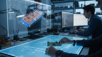
Step-by-Step Process for Designing PCB Layouts
When designing PCB layouts, careful attention to detail and process is vital for ensuring functionality and manufacturability. A well-executed layout can significantly reduce the risk of errors during the PCB printing phase, leading to a higher yield and performance. According to industry reports, nearly 50% of PCB failures can be traced back to design defects, highlighting the importance of a thorough design process. Start by defining your specifications and requirements clearly, taking into context the electrical and mechanical constraints of your application.
One crucial step in the PCB design process is ensuring proper component placement. Components should be organized logically to minimize tracing length and maintain signal integrity. Another essential tip is to utilize a grid system, which helps in aligning components and traces, simplifying the layout process. Data from IPC indicates that optimizing layout can lead to a 30% reduction in manufacturing errors, demonstrating how layout efficiency can directly impact production success.
Effective trace routing is another key consideration. Keeping traces as short and direct as possible helps reduce inductance and capacitance, which can affect performance. To facilitate easier testing and troubleshooting, it is recommended to incorporate test pads and specific routing paths conducive to diagnostics. Adopting these strategies can pave the way for more successful PCB printing, ultimately enhancing product reliability in the competitive electronics market.
Common Challenges in PCB Printing and Their Solutions
When it comes to PCB printing, several common challenges can arise, affecting the quality and efficiency of the process. One significant issue is the alignment of layers during the printing process. Misalignment can lead to defects and compromised electrical connections. To address this, implementing automated alignment systems can significantly reduce human error, ensuring that each layer is accurately placed. Regular calibration of printing equipment is also essential to maintain precision.
Ink viscosity presents another challenge, as it can affect the print quality and the adhesion of the ink to the PCB substrate. Achieving the correct viscosity is crucial for achieving crisp and clear printouts. A practical tip is to regularly monitor the viscosity of the ink and adjust it based on environmental conditions such as temperature and humidity. Using temperature-controlled rooms for printing can enhance consistency in ink performance.
Additionally, underestimating the importance of cleaning procedures can lead to issues like ink clogging and surface contamination. Ensuring that all equipment and substrates are thoroughly cleaned before the printing process can help maintain print quality. Regular maintenance schedules should be established to address potential clogs and ensure the longevity of printing machines. By focusing on these common challenges and their respective solutions, manufacturers can significantly improve their PCB printing techniques.
Innovative Techniques to Enhance PCB Printing Quality
Innovative techniques in PCB printing have revolutionized the way engineers and designers approach circuit board fabrication. One of the most effective methods is the implementation of advanced inkjet printing technology. This method allows for high-resolution printing with minimal waste, enabling designers to create intricate circuit patterns that were once impossible with traditional techniques. By utilizing specialized conductive inks, manufacturers can achieve improved electrical performance and reliability in their final products, significantly enhancing overall PCB quality.
Another innovative approach involves the use of digital direct-to-board printing. This method simplifies the production process by eliminating the need for stencils and screens, thus reducing setup time and costs. Digital printing not only enhances flexibility in design modifications but also allows for rapid prototyping and customization. Leveraging automation and precision control, designers can achieve remarkable accuracy and consistency, which are critical for high-density interconnects and multilayer boards. As the market continues to demand more sophisticated electronic devices, embracing these innovative PCB printing techniques will be essential for maintaining competitive advantages and meeting quality standards.