How to Choose the Right PCB Fabrication Process for Your Project Needs
In the evolving world of electronics, the choice of the right PCB fabrication process is crucial for the success of any project. As technology advances and the demand for more complex electronic circuits increases, understanding the different fabrication techniques becomes essential for designers and engineers alike. Dr. Emily Chen, a leading expert in PCB fabrication with over two decades of industry experience, emphasizes this importance by stating, "Selecting the appropriate fabrication process not only affects the quality and reliability of the circuit board but also influences overall project timelines and costs."
Choosing the right PCB fabrication method requires careful consideration of various factors including design complexity, production volume, and desired material properties. Each fabrication process, whether it be through traditional methods or more advanced, additive techniques, presents unique advantages and potential challenges that can impact the end product. With the right guidance and knowledge, engineers can align their project needs with the most suitable fabrication process, ensuring optimal performance and efficiency. In this article, we will explore key considerations to help you make informed decisions in selecting the right PCB fabrication process for your specific project requirements.

Understanding PCB Fabrication Basics and Terminology
Understanding the basics of PCB fabrication is essential for selecting the appropriate manufacturing process for your project. A printed circuit board (PCB) serves as the backbone of most electronic devices, providing electrical connections and mechanical support for components. The fabrication process typically involves several key steps, such as designing the layout, creating the substrate, etching conductive pathways, and applying surface finishes. Understanding these fundamental stages helps engineers and designers make informed decisions when customizing their PCBs, particularly in relation to functionality, size, and cost.
Terminology is also critical in the PCB fabrication realm. Terms such as "substrate," "layer count," and "via," among others, describe the essential components and structures of a PCB. The substrate refers to the material that supports the circuitry, most commonly fiberglass or epoxy resin. Layer count indicates the number of conductive layers involved in the PCB, which influences the complexity and performance of the board. Vias are small plated holes that facilitate connections between different layers. Familiarity with this terminology not only aids in communication within teams but also enhances the ability to evaluate different fabrication techniques and their suitability for specific project requirements.
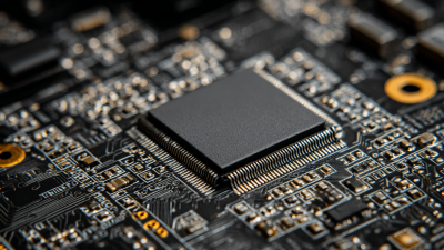
PCB Fabrication Process Comparison
This bar chart compares the costs associated with various PCB fabrication processes. Understanding these costs can help you choose the right process for your project needs.
Identifying Project Requirements and Specifications
Identifying project requirements and specifications is crucial when choosing the right PCB fabrication process. Start by defining the intended application of the PCB. For instance, a consumer electronics project might require a different level of precision and performance compared to a simple hobbyist project. Understand the functional requirements such as power levels, signal integrity, and thermal management. These considerations will guide the selection of materials and design complexity, which are essential for ensuring that the PCB meets the performance standards needed for its application.
Next, consider the physical specifications of the PCB, including size, layer count, and component density. High-density boards with multiple layers may necessitate advanced fabrication techniques, while a simpler design may allow for more straightforward fabrication processes. Additionally, assess the environmental factors that the PCB will encounter, such as temperature fluctuations and exposure to moisture. Understanding these parameters will not only influence material choices but also dictate the manufacturing processes best suited for your project, ensuring reliability and durability in its intended environment. By carefully outlining these requirements and specifications, project managers can streamline the decision-making process, ultimately leading to more successful outcomes in PCB development.
How to Choose the Right PCB Fabrication Process for Your Project Needs - Identifying Project Requirements and Specifications
| Project Type |
Layer Count |
Material Type |
Common Processes |
Typical Lead Time |
Cost Range |
| Consumer Electronics |
2-4 Layers |
FR-4 |
Standard PCB, SMT |
1-3 Weeks |
$500 - $2000 |
| Industrial Equipment |
4-8 Layers |
FR-4, Aluminum |
Multilayer PCB |
3-6 Weeks |
$1500 - $5000 |
| Medical Devices |
6-12 Layers |
Polyimide, Flex |
HDI PCB |
4-8 Weeks |
$2000 - $10000 |
| Aerospace |
8+ Layers |
High-Temperature FR-4 |
Rigid-Flex PCB |
6-12 Weeks |
$5000 - $20000 |
| Automotive |
4-10 Layers |
FR-4, Polyimide |
Standard and Multilayer PCB |
4-8 Weeks |
$3000 - $15000 |
Comparing Different PCB Fabrication Processes
When selecting the right PCB fabrication process for your project, it is vital to compare the different methods available in the industry. The two most common PCB fabrication processes are traditional subtractive manufacturing and additive manufacturing. Subtractive manufacturing involves etching away materials from a board to create the desired circuits, which can be cost-effective for larger production runs. According to a 2022 report by IPC, the global PCB market reached $70 billion, highlighting the widespread reliance on traditional methods, which accounted for approximately 60% of market share due to their proven reliability and efficiency.
On the other hand, additive manufacturing, such as 3D printing, is gaining traction, especially for prototypes and low-volume production. This method allows for the creation of complex geometries and can significantly reduce material waste. A recent study by Gartner indicated that the use of additive manufacturing in PCB production could grow by over 30% annually as technological advancements improve capabilities and reduce costs. When deciding between these processes, it’s essential to consider factors like production volume, complexity of the PCB design, and budget constraints, as each method has its unique advantages and limitations.
Evaluating Cost, Time, and Quality Considerations
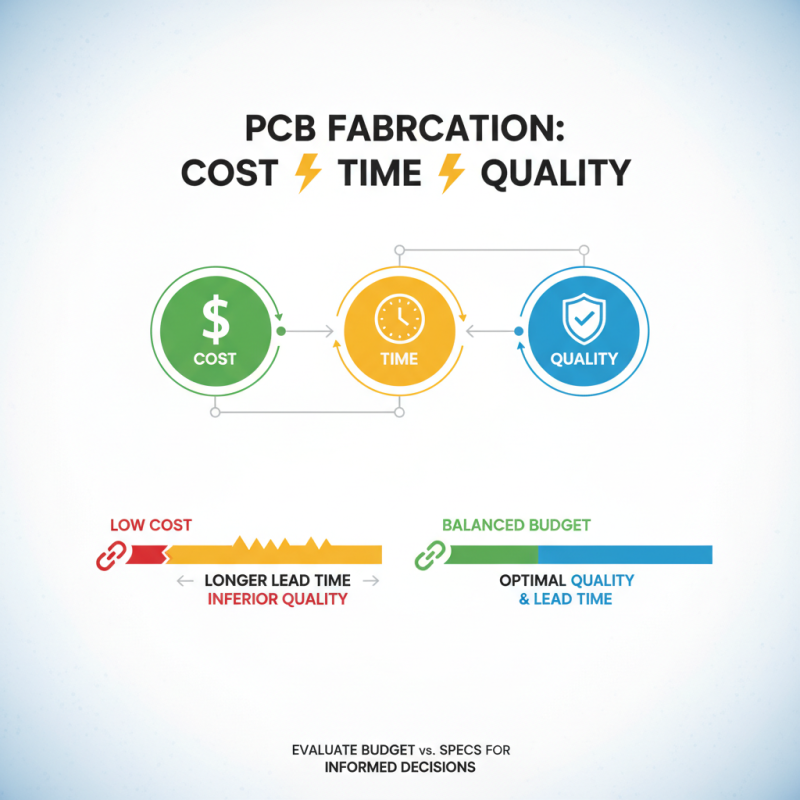
When choosing the right PCB fabrication process, it's crucial to evaluate the interplay between cost, time, and quality. Cost is often the primary consideration, especially for projects with tight budgets. While low-cost options may be tempting, they can lead to inferior quality and longer lead times due to potential reworks. Understanding the balance between your budget and the required specifications will help in making informed decisions.
Time efficiency also plays a crucial role in PCB fabrication. Rapid prototyping methods can significantly speed up the development process, allowing for quicker iterations and enhancements. However, these expedited services may come at a premium. Assessing your project's timeline against the urgency of your deliverables will guide you in selecting the appropriate fabrication process that aligns with your scheduling needs.
Tips: Always consider the long-term implications of your choice. Opting for a slightly more expensive fabrication process might yield higher quality boards that reduce troubleshooting and maintenance costs down the line. Additionally, seek feedback from peers or consult with fabrication specialists to better understand the trade-offs involved in your selections. This approach will result in more reliable and successful outcomes for your projects.
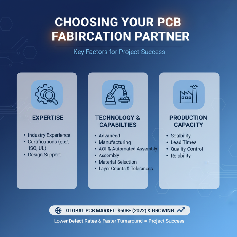
Selecting the Ideal PCB Fabrication Partner
Choosing the right PCB fabrication partner is crucial for the success of any electronic project. The global PCB market was valued at over $60 billion in 2022 and is projected to grow significantly in the coming years, highlighting the increasing demand for quality fabrication services. When selecting a partner, it’s essential to consider their expertise, technology capabilities, and production capacity. Industry reports indicate that companies with advanced manufacturing processes, such as automated optical inspection (AOI) and automated assembly, tend to achieve lower defect rates and faster turnaround times, which are vital for maintaining project timelines.
Additionally, understanding the partner’s certifications and quality management systems is critical. According to IPC standards, a reputable PCB manufacturer should adhere to stringent quality control processes to ensure reliability and performance. Selecting a fabrication partner that holds certifications like ISO 9001 and IPC-A-600 can offer assurance of their commitment to quality and customer satisfaction. Furthermore, it’s beneficial to assess their communication practices and customer support, as these factors significantly impact project collaboration and overall success. Engaging with a partner who prioritizes transparency and responsiveness can save time and reduce complications down the line, leading to a smoother product development process.