How to Create a PCB Prototype for Your Electronics Project?
Creating a PCB prototype is a critical step in bringing electronics projects to life. Experts like Dr. Emily Chen, a leading figure in PCB design, emphasize, “A well-crafted prototype can save time and resources in the long run.” This statement highlights the significance of getting your PCB prototype right.
When starting your project, consider your design clarity and purpose. Each component on the PCB should have a specific function. Mistakes at this stage can lead to costly revisions later. Sometimes, it's easy to overlook design complexities. Simplicity often yields stronger functionality.
Additionally, prototyping involves testing and revising. Not every prototype will work as expected. In fact, the first version might uncover flaws in the design. Embracing this iterative process is essential for improvement. Overall, the ability to learn from the mistakes in your PCB prototype will ultimately lead to a more successful final product.
Understanding the Basics of PCB Prototyping for Electronics Projects
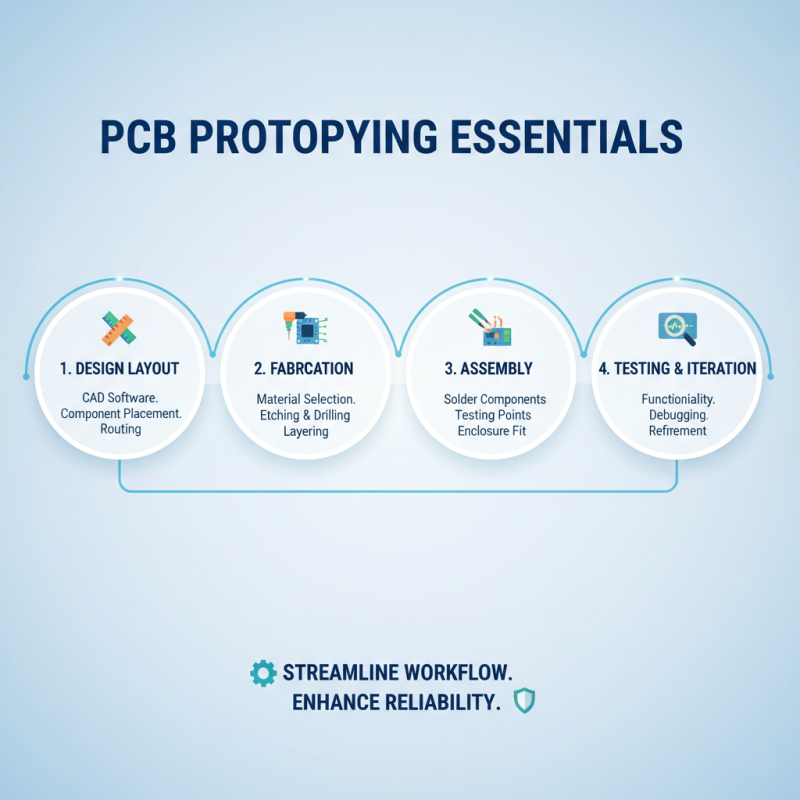
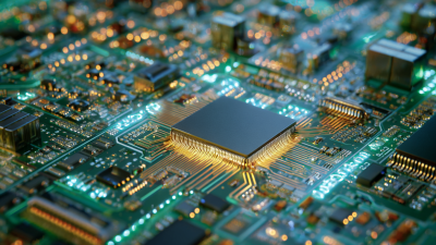
PCB prototyping is a vital step in electronics projects. Understanding the basics helps streamline your workflow. It also enhances the final product’s reliability. A printed circuit board (PCB) connects various electronic components. Proper layout design is crucial for performance.
Begin by sketching your circuit design. Use software tools to translate sketches into digital formats. Remember to label each component clearly. Overlapping traces can lead to short circuits. A clean layout minimizes errors. During the design phase, review your work. Ask peers for feedback on your design. Mistakes here can be costly.
Once you have your design, it's time for fabrication. Choose a service based on your needs. Verify the specifications required for your project. Often, there's a trade-off between cost and quality. If your prototype doesn't function, it’s a learning opportunity. Each error teaches valuable lessons. Reflect on what went wrong and improve your process. Adjustments in design or layout can lead to success. Embrace this iterative process; it’s part of PCB prototyping.
Choosing the Right PCB Design Software for Your Prototype
Choosing the right PCB design software is crucial for your prototype's success. Several options cater to different skill levels. Some are straightforward for beginners, while others boast advanced features for professionals. Consider your experience and project needs when making a choice.
Tip: Always test the software with simpler projects. This helps you understand its features and workflow. You might encounter challenges, like a steep learning curve or limited resources. Don't hesitate to seek help from online communities or tutorials.
When selecting software, look for intuitive interfaces and helpful customer support. Even well-reviewed tools can have quirks. You could find that a widely recommended option doesn’t suit your style. Experiment with different tools until you find the right match. Your choice can significantly impact your design process.
How to Create a PCB Prototype for Your Electronics Project? - Choosing the Right PCB Design Software for Your Prototype
| Software Name |
Key Features |
Target Users |
Pricing Model |
| Eagle |
User-friendly interface, schematic editor, and PCB layout tools |
Hobbyists and small businesses |
Subscription or pay-per-use |
| KiCad |
Open-source, multi-platform, supports 3D viewer |
All levels, especially for users favoring open-source |
Free |
| Altium Designer |
Advanced routing, design rule checks, and simulation tools |
Professional engineers and designers |
Subscription-based |
| Fusion 360 |
Integrated CAD, CAM, and PCB design |
Designers and engineers |
Subscription |
| EasyEDA |
Web-based, schematic capture, PCB layout, and simulation |
Hobbyists and students |
Freemium |
Step-by-Step Guide to Designing Your PCB Layout
Creating a PCB layout can be a challenging yet rewarding process. Start by sketching your circuit. Use graph paper to visualize the components and their connections. A rough diagram helps in understanding the overall flow of the circuit. Don’t aim for perfection at this stage; focus on getting your ideas down.
Next, use PCB design software to create your layout. Many tools are available for beginners. Import your sketch and begin to place components on the board. Pay attention to the spacing. Components should not be too close together, or you may face soldering difficulties later. It’s common to realize that you’ve made errors, or that your design doesn’t quite fit. Don’t get discouraged; iterative design is part of the process.
As you finalize your design, consider the routing of tracks. Keep them short and avoid sharp angles. Too many turns can affect performance. After completing the layout, review it thoroughly. Mistakes often slip through the cracks, especially when you are too close to the work. Seek feedback from peers; fresh eyes can catch what you overlooked. Refine your design based on their suggestions. This ensures a smoother path to creating your prototype.
Component Usage in PCB Prototyping
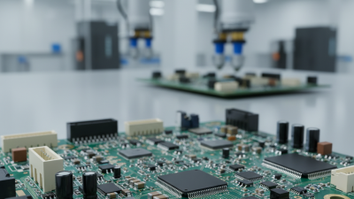
Fabrication Options for PCB Prototyping: What to Consider
When considering PCB prototyping, fabrication options play a crucial role. Different methods can impact the quality and speed of production. For instance, standard PCB fabrication typically takes 1-2 weeks, while advanced techniques like 3D printing may reduce this to just a few days. However, 3D printing can introduce challenges like limited materials and precision issues.
It’s important to weigh the trade-offs. Traditional methods often support complex multilayer boards. According to industry reports, nearly 65% of engineers reported using standard fabrication for affordable prototypes. That being said, the cost can escalate quickly. A basic PCB prototype may cost as little as $10, but advanced features can push prices to $200 or more.
Design for manufacturability is another factor to evaluate. Factors like hole sizes, trace widths, and layout can affect final production results. Nearly 70% of PCB prototypes require redesigns due to manufacturability issues. Balancing innovation with practicality remains a challenge for many designers. Careful consideration of your fabricating method is essential for project success.
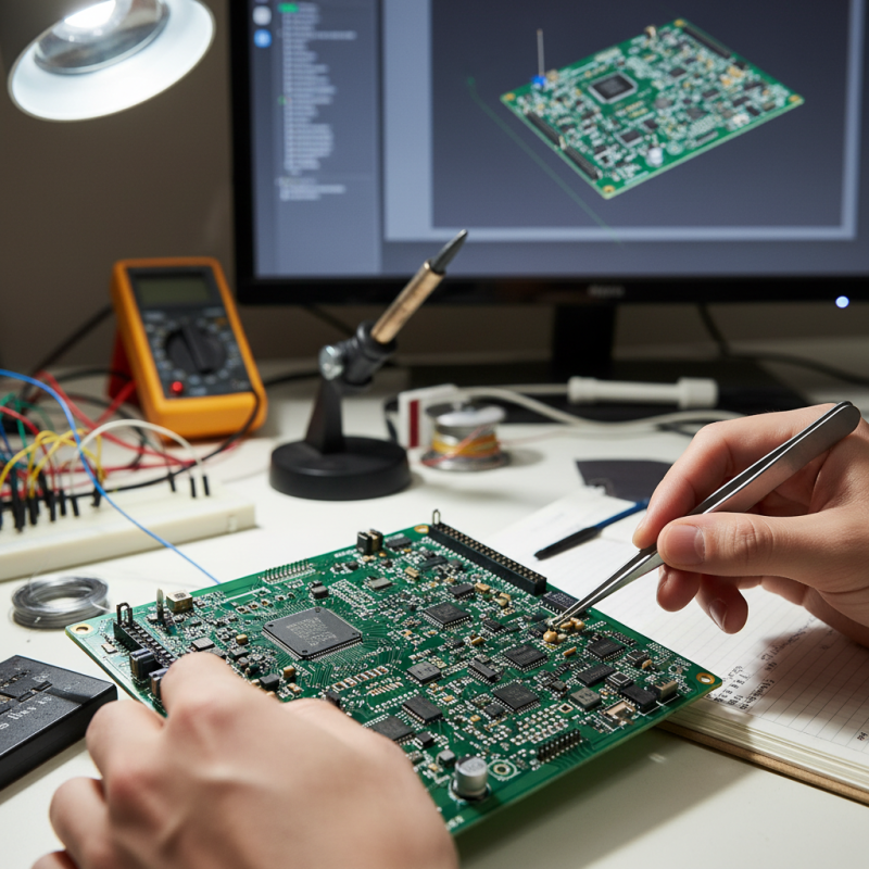
Testing and Troubleshooting Your PCB Prototype Before Finalization
Testing a PCB prototype is crucial for identifying flaws and optimizing the design. According to a recent industry report, nearly 65% of electronic projects encounter issues during the prototyping phase. These problems can range from simple connectivity errors to complex circuit malfunctions. A thorough testing process helps catch these issues before finalization.
Start by conducting visual inspections. Check for soldering defects, misplaced components, and signs of overheating. It’s essential to use a multimeter to test for continuity. If the circuit doesn’t behave as expected, run simulations. Often, it is the overlooked details that cause significant setbacks. Document any inconsistencies you find right away.
Troubleshooting is an iterative process. If you miss an issue during initial testing, it may lead to project delays. In practice, 70% of engineers report revisiting their designs based on test feedback. Use prototype feedback to refine processes and components. A willingness to adapt your design is key to successful outcomes. Embrace the learning curve; mistakes can pave the way for improvement.