Top 10 Tips for Successful PCB Board Design Techniques and Best Practices
In the realm of electronics, successful PCB board design is crucial. As technology evolves, it becomes more complex. Designers face challenges such as component placement and signal integrity. These aspects are essential for performance and reliability. A flawed design can lead to costly failures. Each decision impacts the final product.
PCB board design requires careful consideration of various factors. Every layer must be optimized. The layout should minimize interference while ensuring efficiency. Choosing the right materials is also important. Some designers overlook these details, leading to issues later. Small mistakes can snowball into major problems.
The journey of PCB board design is a learning experience. Designers often reflect on their past projects. They recognize what worked and what didn’t. Embracing best practices can reduce risks. Ultimately, a well-designed PCB can make a significant difference in product success.
Understanding PCB Design Fundamentals and Terminology
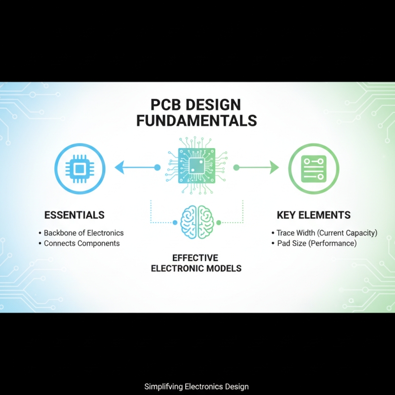
Understanding PCB design fundamentals is essential for creating effective electronic models. A printed circuit board (PCB) is the backbone of electronic devices. It connects different components and facilitates functionality. Designers must grasp key terms, such as trace width and pad size. These influence current capacity and overall performance.
Another important concept is layer count. Single-layer boards are simpler but limited. Multi-layer designs offer complexity but require meticulous planning. Also, consider design rules like clearance and drill sizes. Ignoring these can lead to costly errors. Reflect on your choices; even experienced designers make mistakes.
Moreover, component placement is crucial. A well-organized layout minimizes noise and interference. Yet, many overlook this step and face challenges later. Every design choice matters and can affect the final product. Experimentation is vital. Learning from failures leads to better designs. It’s a journey of continuous improvement.
Essential Design Tools and Software for PCB Development
When designing a PCB, the choice of tools and software is crucial. Many designers rely on CAD software for layout and schematics. A recent industry report indicated that about 45% of PCB professionals prefer using advanced simulation tools. These tools help visualize potential issues, yet many designers still overlook them. Not using simulation can lead to errors in thermal performance or signal integrity.
Furthermore, collaboration tools are gaining traction in the PCB design process. Approximately 30% of teams now utilize cloud-based platforms for real-time updates. These platforms allow team members to share files easily. However, reliance on cloud tools can present challenges. Slow internet speeds may hinder workflow and lead to frustration.
Prototyping tools are also essential for PCB development. Many engineers construct physical prototypes to test their designs. While this approach is beneficial, it can be time-consuming and costly. Over 60% of PCB projects exceed budget due to multiple prototype iterations. It's a reminder that effective planning can mitigate excessive expenses in the design stage.
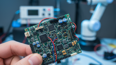
Key Considerations for Layout and Component Placement
When designing a PCB, layout and component placement are crucial. Start by prioritizing the flow of signals. Arrange components to minimize trace lengths. This reduces noise and enhances performance. However, achieving the perfect layout is often a challenge. Consider how components interact, as this can affect the entire circuit.
Spacing is another key aspect. Keep sensitive components away from noisy ones. This might mean compromising on compactness. Some designers overlook the importance of thermal management. Ensure that heat-generating components have proper spacing and cooling paths. This choice can lead to potential failures if not done right.
Lastly, documentation is vital. Maintain clear records of your design choices. These notes can highlight areas for improvement in future projects. It's easy to skip this step, but reflecting on your design process can offer invaluable insights. Mistakes happen, but acknowledging them leads to better designs down the line.
Best Practices for Signal Integrity and Power Distribution
Signal integrity and power distribution are crucial aspects of PCB design. Ensuring the reliability of signals requires careful consideration. Minimize trace lengths as much as possible. Shorter traces reduce the chance of interference. Use ground planes to shield critical signals. They help maintain a stable reference.
Power distribution needs attention, too. Planning the power supply routes can prevent voltage drops. Thick traces and adequate vias are essential. Use decoupling capacitors near power pins. This approach stabilizes voltage and improves performance. Avoid placing sensitive components close to noisy circuits. Noise can disrupt signal integrity.
Reflection should be part of your design process. After creating a layout, evaluate it for potential issues. Simulate the design for signal integrity using software tools. Check trace widths against current requirements. Small errors can lead to significant problems in functionality. Remember, PCB design involves constant learning and improvement. Each project brings new challenges and lessons.
Top 10 Tips for Successful PCB Board Design Techniques and Best Practices
| Tip Number |
Design Technique |
Description |
Best Practice |
| 1 |
Layer Stack-up |
Use an appropriate stack-up configuration for impedance control. |
Maintain a consistent layer thickness and type. |
| 2 |
Signal Routing |
Route high-speed signals on inner layers. |
Avoid vias on critical signal paths. |
| 3 |
Ground Plane |
Use a solid ground plane to reduce EMI. |
Connect all ground components to this plane. |
| 4 |
Decoupling Capacitors |
Place decoupling capacitors close to IC power pins. |
Use multiple capacitor values for better performance. |
| 5 |
Thermal Management |
Incorporate heat sinks and thermal vias for hot components. |
Monitor thermal performance in layout stage. |
| 6 |
Impedance Control |
Follow guidelines for controlled impedance traces. |
Use calculators or simulation tools for precise values. |
| 7 |
Design Rule Check (DRC) |
Conduct thorough DRC to catch errors early. |
Perform multiple checks at different design stages. |
| 8 |
Via Management |
Optimize via placements to minimize inductance. |
Use blind/buried vias where applicable. |
| 9 |
PCB Thickness |
Select the right thickness based on mechanical strength. |
Consider stacking multiple boards for thickness adjustment. |
| 10 |
Final Review |
Conduct a comprehensive review before production. |
Involve multiple team members for feedback. |
Effective Testing and Prototyping Techniques for PCBs
Effective testing and prototyping techniques are crucial for successful PCB design. Iterative testing helps identify weaknesses early in the design phase. Build small prototypes to evaluate component placement and circuit performance.
This hands-on approach often reveals issues that simulations may miss. Checking for component clearance and soldering points in real life is essential.
When testing, consider environmental variables. Temperature changes can affect performance. Place prototypes in different settings to observe behavior. Make adjustments based on these real-world tests. Think critically about the results. Sometimes, components work well in theory but fail in practice. A simple adjustment might solve a complex failure.
Don't underestimate the value of feedback. Collaborate with team members to review prototypes. Different perspectives can highlight overlooked problems. Document every step of your testing process. This record helps refine the design on future iterations. Addressing faults as they arise can lead to a more robust final product.