
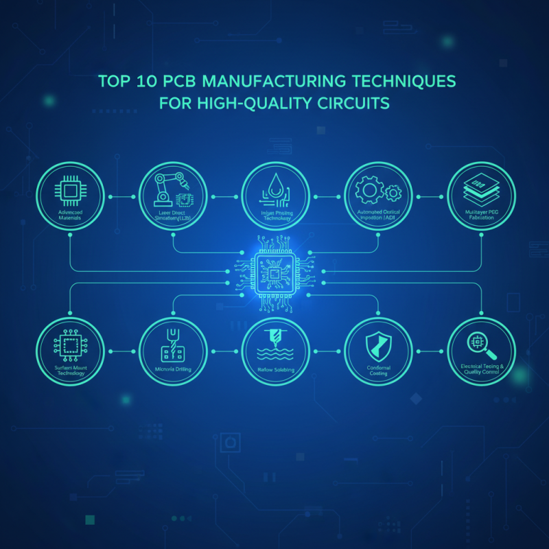
Top 10 PCB Manufacturing Techniques You Need to Know for High Quality Circuits
In the realm of electronics, the importance of high-quality circuit boards cannot be overstated. PCB manufacturing plays a crucial role in the performance, reliability, and longevity of electronic devices. As technology continues to evolve, manufacturers are constantly seeking innovative techniques to enhance the quality and efficiency of their production processes. Understanding the various PCB manufacturing techniques is essential for anyone involved in the design and production of circuits, whether in a commercial capacity or as a hobbyist.
This article delves into the top 10 PCB manufacturing techniques that are integral to achieving superior circuit quality. From advanced materials to cutting-edge fabrication methods, we will explore the best practices that can elevate the standard of PCB creation. By adopting these techniques, manufacturers can not only improve the functionality of their products but also keep pace with the increasingly competitive landscape of electronic manufacturing. Join us as we uncover the essential approaches that every PCB designer and manufacturer should be aware of to ensure their circuits meet the highest quality standards.
Overview of PCB Manufacturing Techniques for Quality Circuits
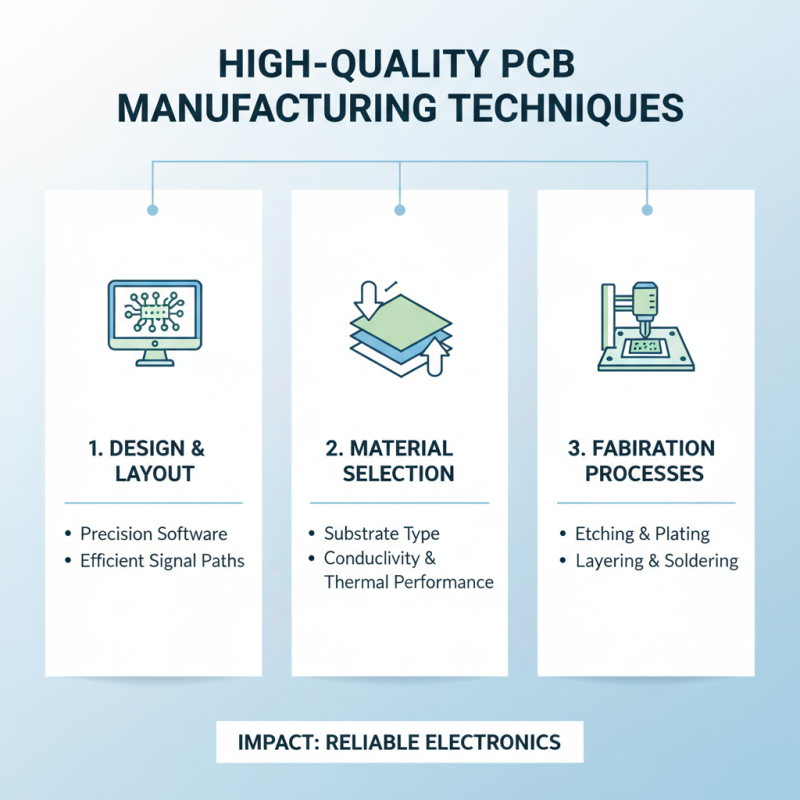
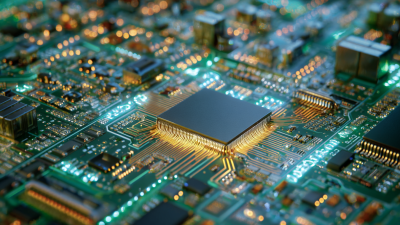
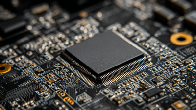
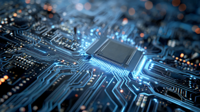
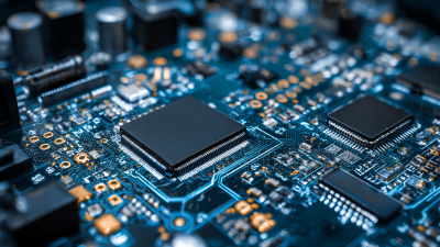
In the realm of electronics, the quality of printed circuit boards (PCBs) significantly impacts the overall performance of devices. Understanding various PCB manufacturing techniques is essential for ensuring high-quality circuits. The process starts with precise design and layout using specialized software, which is crucial for creating efficient paths for electrical signals. This design phase must include considerations for the materials used, as different substrates can affect conductivity and thermal performance.
Once the design is finalized, the manufacturing process typically involves several key techniques. These include etching, which removes unwanted copper from the board to form the circuit layout, and lamination, where multiple layers are fused together for complex circuits. Additionally, the techniques of solder mask application and surface mount technology are vital for protecting the boards and facilitating the assembly of components. Each of these methods requires meticulous attention to detail and adherence to specific standards to produce PCBs that are not only functional but also reliable in demanding applications. By mastering these techniques, manufacturers can enhance the quality and longevity of their circuits, ultimately leading to superior product performance.
Related Posts
-
Top 10 Tips for Efficient Circuit Board Manufacturing Process Optimization
-
Top 5 US Based PCB Manufacturers to Watch in 2025
-
Transforming Industries: The Future of PCB Production and Its Impact on Technology
-
Unlocking Efficiency: The Future of PCB Production Techniques in Modern Electronics
-
Understanding the Impact of Printed Circuit Board Assembly on Today's Electronics Industry and Market Growth
-
Innovative Trends in PCB Printing That Will Transform the Electronics Industry