What Is PCB Printing and How Does It Work?

A circuit board may look like a flat green sheet, but it carries a carefully planned electrical map. PCB printing is the process of transferring circuit patterns onto a laminate panel. The goal is not decoration. It is accurate conductivity. Tiny details matter.

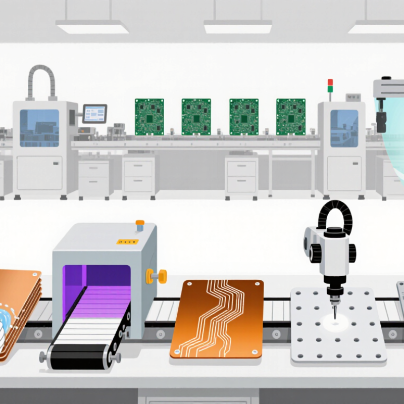
In practical production, engineers begin with digital design files. A copper-clad panel is cleaned before applying photoresist. Ultraviolet light exposes the required pattern. Chemical etching then removes unwanted copper. Holes are drilled, plated, and checked for reliable connections. A solder mask protects the surface, while silkscreen markings identify components. Each stage affects alignment, resistance, and durability. A small dust particle can create an open circuit. Poor registration can connect tracks that should remain separate. These faults may appear much later. That makes inspection essential.

This guide explains how PCB printing works, from pattern transfer to final testing. It connects production methods with practical quality checks and safety-conscious handling. Terminology can vary between manufacturers. Some companies use “printing” broadly, while others separate imaging, etching, and marking. The distinction is easy to miss. There is no single production recipe. Board thickness, layer count, materials, and order volume all change the process. A simple prototype may require different equipment from a high-volume production line. Understanding these differences helps readers assess technical claims, compare suppliers, and ask better questions. The process can seem mechanical. It still depends on disciplined decisions.
What Is PCB Printing and How Does It Work?

What PCB Printing Means and What It Produces

PCB printing is the process of turning a circuit design into a physical printed circuit board. It does not mean printing a finished electronic device. Instead, it creates conductive copper paths on an insulating base, often with several layers joined together. These paths connect component locations, such as small circular solder pads, while keeping signals on planned routes. That distinction matters. The result is usually a bare board, not a board populated with chips or connectors.

Tips: Check the layer count, board thickness, and copper weight before production. A clear design file helps prevent misplaced holes or narrow traces. Small errors travel.

The finished board may also include a protective solder mask and printed labels that mark component positions. These features make assembly and inspection easier. Manufacturing can involve imaging, etching, drilling, and plating, with checks for trace spacing and electrical continuity. The exact steps depend on the board’s design. The word “printing” can be misleading; it describes pattern transfer, not ordinary ink on paper. A useful specification should describe the physical board and its tolerances, not just the artwork.

What Is PCB Printing and How Does It Work? — What PCB Printing Means and What It Produces

Dimension What It Means How It Works What It Produces
PCB printing A common term for forming conductive circuit patterns on a printed circuit board. It usually describes a sequence of fabrication steps rather than printing the entire board in one operation. A circuit design is transferred to copper-clad material, then unwanted copper is removed or conductive material is deposited, depending on the manufacturing method. A board with conductive paths that connect electronic components according to the circuit design.
Design transfer The process of transferring the board’s circuit layout onto a copper layer. For many conventional boards, a photoresist layer is exposed through a patterned image and developed. Other methods may use direct imaging or printed etch-resistant ink. A protected copper pattern that defines which areas will remain as circuit traces.
Copper patterning The creation of traces, pads, and other conductive features from a copper layer. In subtractive fabrication, exposed copper is chemically etched away while protected copper remains. The resist is then removed. Visible copper tracks and connection pads arranged to match the board layout.
Board material The insulating base that supports the copper circuitry. Copper foil is bonded to a rigid or flexible insulating substrate. A widely used rigid-board substrate is glass-fiber-reinforced epoxy laminate. A mechanically supported circuit layer, or multiple layers when copper and insulating layers are laminated together.
Multilayer construction A board structure containing multiple patterned copper layers. Inner circuit layers are patterned, stacked with insulating material, and laminated. Drilled holes and plated connections can link selected layers. A compact board with electrical routing on more than one copper layer.
Drilling and plated holes Holes used for component leads or electrical connections between board layers. Mechanical or laser drilling creates openings. In plated through-holes, a conductive copper layer is deposited on the hole walls. Mounting or lead holes, and—where plated—electrical paths between copper layers.
Solder mask A protective coating applied over much of the copper surface. The coating is patterned to leave selected pads exposed for soldering. Insulation over covered areas that helps protect copper and reduce the risk of solder bridging.
Legend or silkscreen Printed identification and assembly markings on the board surface. Text, component outlines, polarity marks, or reference labels are applied as a separate marking step. Labels that help identify components and support assembly, inspection, and servicing.
Inspection and electrical testing Checks that the manufactured board matches its design and has the required connections. Manufacturers may inspect features optically and test electrical continuity or isolation between specified points. A verified bare PCB ready for electronic components to be mounted and soldered.
PCB “printing” typically refers to producing patterned conductive features and related board layers; it does not necessarily mean using an ordinary paper printer.

The Main Materials and Layers Used in a Printed Circuit Board

What Is PCB Printing and How Does It Work?

A printed circuit board is built from carefully bonded materials, not ordinary paper. The base is usually FR-4, a glass-fiber weave held in epoxy resin. It provides stiffness, electrical insulation, and heat resistance. Flexible boards often use polyimide instead. Copper foil forms the conductive paths. Typical copper thickness ranges from 18 to 35 micrometres on standard layers.

A multilayer board alternates copper layers with dielectric sheets called prepreg. Heat and pressure cure the prepreg, creating a solid stack. Drilled holes, called vias, connect selected copper layers. The board may contain four, eight, or more layers. IPC-2221 design guidance helps engineers control spacing, current capacity, and insulation distances. According to the Global Electronics Association’s 2024 production analysis, Asian facilities represented more than 90% of global PCB production by value in 2023. That concentration makes material consistency especially important.

PCB printing begins with imaging the circuit pattern onto copper. Unwanted copper is etched away, then the exposed tracks may receive additional plating. A solder mask covers most copper and leaves pads visible. It is usually green, but other colors exist. A printed legend identifies components and polarity. Surface finishes, such as electroless nickel immersion gold or lead-free protective coatings, improve solderability. Prismark’s 2024 industry analysis places annual global PCB sales in the tens of billions of dollars, reflecting enormous manufacturing scale. Yet scale does not remove weak points. A small registration error can misalign layers. Engineers still need to question familiar stackups, because “standard” materials can behave differently under heat and moisture.

How Circuit Designs Become PCB Production Files

A PCB begins as a circuit idea, often drawn as a schematic. The schematic shows electrical relationships, not physical shape. Engineers then assign footprints to each component, such as a small pad pattern for a resistor or a larger outline for a connector. This step needs care. A correct symbol with the wrong footprint can ruin an otherwise sound design.

The layout process turns those relationships into copper geometry. Designers place components, route traces, define board layers, and set clearances for manufacturing. Power paths may need wider traces, while sensitive signals require controlled spacing. A practical review checks connector locations, mounting holes, thermal areas, and access for inspection. The board should make sense in someone’s hands, not only on a screen.

Before production, the design database is converted into manufacturing files. Gerber or similar files describe copper, solder mask, and silkscreen layers. Drill files define plated and unplated holes. Assembly production also needs a bill of materials, component coordinates, and placement direction data. Manufacturing engineers run design rule checks and compare the output against the original schematic. They may find a missing solder mask opening or an unclear reference label. Small errors matter. A final visual review remains valuable, because automated checks cannot understand every real-world assembly problem.

The Step-by-Step PCB Printing and Etching Process

What Is PCB Printing and How Does It Work?

The Step-by-Step PCB Printing and Etching Process

PCB printing transfers a circuit pattern onto copper-clad board; it does not print copper itself. The pattern is prepared with circuit-design software, then printed onto transparent film as a dark mask. For photoresist boards, clean the copper surface and apply the light-sensitive layer evenly. Dust matters. A tiny speck can interrupt a narrow trace.

Align the film over the board and expose it to ultraviolet light. The mask shields the copper areas intended to become circuit paths. Develop the board according to the resist instructions, revealing copper that should be removed. Place it in a suitable etching solution and gently agitate the container. Uncovered copper gradually disappears, while protected copper remains. Rinse thoroughly, then remove the resist. Wear eye protection and gloves, and follow the chemical’s handling instructions.

Inspect the traces under bright light before drilling component holes. Look for breaks, copper bridges, and edges that appear ragged. A basic continuity test can catch a hidden open circuit. If a trace is too thin, adjust the artwork and repeat the process. It is tempting to blame the etchant, but poor cleaning or film alignment can cause the same defect. That part takes practice.

How Finished PCBs Are Inspected and Prepared for Assembly

Finished PCB inspection begins after fabrication, but before components arrive. Operators first check board dimensions, layer registration, surface finish, solder mask, and drilled holes. A calibrated optical system compares copper patterns with the approved design file. It can reveal open traces, shorts, pinholes, scratches, and incomplete pads.

Electrical testing then checks continuity and isolation between nets. Flying-probe testing suits smaller batches, while fixture testing supports repeated production. Inspectors also review impedance reports, cross-sections, and plating thickness. IPC-A-600 and IPC-6012 provide widely used acceptance and qualification guidance. The Global E-waste Monitor 2024 reported 62 million tonnes of electronic waste in 2022, with only 22.3% formally collected and recycled. Better inspection can reduce avoidable scrap, though it cannot fix poor design decisions.

Tips: Keep the fabrication drawing, drill file, and revision code beside the inspection record. Confirm critical dimensions with actual gauges, not eyesight. Clean boards before testing; flux residue can imitate contamination or leakage. For assembly preparation, package boards in dry, sealed materials when moisture sensitivity matters. Check warpage on a flat surface, then verify fiducials, tooling holes, and panel edges. A final review should confirm that labels remain readable and solderable areas are undamaged. I still find visual checks reassuring, but they are not enough. People miss tiny defects.、】【