What Is PCB Production and How Does It Work?
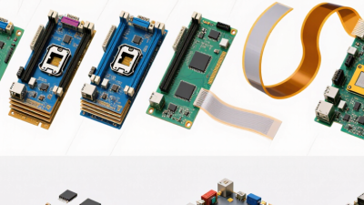
PCB production is the controlled process of turning an electrical design into a reliable circuit board. These boards connect components through copper pathways, insulated layers, and carefully placed holes. They appear in phones, vehicles, medical devices, industrial controls, and everyday appliances.
A board usually begins with a schematic and a digital layout. Engineers define trace widths, spacing, layer arrangements, and component locations. The design is transferred onto copper-clad laminate, often fiberglass-reinforced epoxy. Imaging exposes the circuit pattern, while chemical etching removes unwanted copper. Drilling creates openings for component leads and plated vias. These tiny connections join different layers. Small details matter.
The process continues with copper plating, solder mask application, surface finishing, and printed reference marks. Some manufacturers then assemble components using automated placement and reflow soldering. Quality teams inspect the board with automated optical systems, microscopes, and electrical tests. Standards such as IPC guidance help manufacturers control workmanship and consistency. However, compliance alone does not guarantee perfect performance. Material variation, trapped moisture, contamination, or inaccurate drilling can still create failures.
Reliable PCB production depends on documented procedures, trained operators, suitable equipment, and honest testing records. Experienced manufacturers monitor temperature, chemical concentration, line width, and hole quality throughout production. They also review design-for-manufacturing risks before fabrication begins. A practical review may reveal a trace that is technically valid but difficult to produce repeatedly. That lesson is easy to overlook. Understanding each stage makes it easier to judge board quality, compare suppliers, and prevent costly redesigns before production starts.

What PCB Production Means and Why It Matters
What Is PCB Production and How Does It Work?
What PCB Production Means and Why It Matters
PCB production turns an electrical design into a physical circuit board. Engineers begin with copper-clad laminate, then create circuit images through photoimaging or laser direct imaging. Chemical etching removes unwanted copper, leaving precise conductive paths. Drilling forms holes for component leads and interlayer connections. Plating strengthens those holes with copper.
The process continues with solder-mask coating, surface finishing, printing, and electrical testing. A technician may inspect a tiny via under magnification, checking for cracks, residue, or incomplete plating. These details matter because a small defect can interrupt power, signal timing, or heat dissipation. IPC’s 2024 PCB Technology Roadmap highlights rising demands for finer lines, higher layer counts, and better thermal control. Production is becoming less forgiving.
The economic impact is substantial. Fortune Business Insights estimated the global PCB market at about 89.7 billion dollars in 2023, with continued growth expected through the decade. That growth reflects expanding demand for electronics in transport, medical equipment, communications, and industrial automation. Yet production is not perfectly efficient. It consumes chemicals, water, energy, and raw materials. Better process control can reduce scrap, but every factory faces trade-offs between speed, cost, and reliability. That admission matters. A board should not be judged only by appearance; traceability, testing records, material quality, and long-term performance are equally important.
What Is PCB Production and How Does It Work?
PCB production converts copper-clad laminate into a finished circuit board through imaging, etching, drilling, plating, solder-mask application, and electrical testing. Copper thickness is a key production parameter because it affects current-carrying capacity, heat dissipation, and manufacturing cost.
The chart shows common nominal copper thicknesses used in PCB manufacturing. One ounce of copper is approximately 35 micrometres thick; heavier copper is selected for higher-current or better thermal-performance applications. Actual finished thickness can vary because of plating and etching processes.
Core Materials and Design Preparation for PCB Manufacturing
What Is PCB Production and How Does It Work?
Core Materials and Design Preparation for PCB Manufacturing
PCB production starts with a controlled stack of materials. The core usually contains woven glass fabric and resin. Copper foil forms the conductive layers. A solder mask protects exposed copper from oxidation and accidental bridging. Surface markings identify components during assembly and inspection.
Material selection affects electrical, thermal, and mechanical performance. High-speed circuits may require a substrate with stable dielectric properties. Power boards often need thicker copper and stronger thermal management. Layer count, board thickness, and copper weight should be defined before routing begins. Small details matter.
Design preparation begins with a verified schematic and a clear layer stackup. Engineers set trace widths, spacing, via sizes, and impedance targets. They also check return paths around fast signals. Manufacturing rules should guide the layout, not correct it afterward. A design-rule check can catch narrow gaps, trapped copper, and unconnected nets.
File preparation must include accurate fabrication data, drill information, and controlled tolerances. Notes should explain critical dimensions and surface requirements. In practice, a clean design file is not always a manufacturable one. I have seen layouts pass electrical checks but fail assembly clearance review. That weakness deserves reflection. Prototype feedback can reveal heat concentration, difficult probing, or fragile edge features before production expands.
How Circuit Patterns Are Transferred to the Board
What Is PCB Production and How Does It Work?
How Circuit Patterns Are Transferred to the Board
The board starts bare. A copper-clad laminate provides the flat base for the circuit. Its surface must be clean, dry, and free from fingerprints. Even a tiny particle can interrupt a narrow trace. In practice, preparation often determines the quality of later imaging.
Manufacturers apply a light-sensitive film called photoresist over the copper. A circuit layout is placed above the film, using precise registration holes for alignment. Ultraviolet light hardens selected areas of the resist. Some production lines use direct imaging instead of a physical pattern film. Alignment matters. Small errors spread.
After exposure, a developer removes the unprotected resist and reveals parts of the copper. The board then enters an etching process. Chemical solution dissolves the exposed copper while the protected areas remain as circuit paths. Technicians control temperature, spray pressure, and solution strength. Poor control can make traces too thin or leave unwanted copper bridges.
The remaining resist is stripped away, leaving the transferred pattern visible. Drilling creates holes for component leads and electrical connections between layers. Plating may reinforce hole walls and add copper thickness to working surfaces. Automated inspection checks spacing, openings, and registration. Human review still helps identify dull patches, scratches, or unusual discoloration. The process is highly controlled, but not flawless. A board can pass early checks and still require deeper testing for continuity, insulation, and dimensional accuracy.
Layer Assembly, Drilling, Plating, and Surface Finishing
PCB production turns circuit drawings into a controlled stack of copper, dielectric, and protective materials. Layer assembly starts with inner copper foils and insulating sheets. Engineers align each layer with registration targets. Heat and pressure bond the stack into one panel. Tiny shifts matter. A misplaced layer can change impedance or break a connection. In my experience, clean handling is as important as precise equipment. Dust, moisture, and hurried alignment often create defects that appear much later. The process seems orderly, but it is not perfectly forgiving.
After lamination, CNC drilling creates through-holes, vias, and mounting holes. Tool wear must be monitored, because a dull bit can smear resin or leave rough walls. Hole quality affects electrical reliability. Desmearing prepares the walls for plating. Chemical treatment deposits a thin conductive layer inside each hole. Electroplating then builds copper to the specified thickness on surfaces and hole walls. Operators check current density, bath condition, and panel movement. Small variations are easy to underestimate.
Surface finishing protects exposed copper and supports dependable soldering. Common finishes include immersion tin, electroless nickel with a gold layer, and organic coatings. The correct choice depends on storage time, assembly temperature, contact use, and cost. Inspection includes coating thickness, solderability, drill accuracy, and electrical continuity. Automated inspection helps, but it cannot replace process judgment. A test result may pass while a weak control trend goes unnoticed. Production teams should pause, review records, and improve the next panel.
Inspection, Testing, and Final PCB Quality Control
During PCB production, quality control begins before the board reaches final assembly. Inspectors examine copper patterns, drilled holes, solder masks, and component placement. Under bright lighting, they look for scratches, exposed copper, uneven coatings, and blocked vias. Automated optical inspection compares each board with approved design data. However, software can miss unusual shadows or subtle surface damage. Human review remains necessary.
Electrical testing checks whether current follows the intended paths. Continuity testing confirms that connected points conduct electricity. Isolation testing checks for unwanted connections between separate circuits. Functional testing may power the finished board and measure voltage, signal timing, and response. Test fixtures must fit accurately, or false failures can appear. That detail is easy to underestimate.
Final PCB quality control combines inspection records, test results, and production traceability. Teams should verify calibrated instruments, clear acceptance criteria, and controlled storage conditions. Moisture, dust, and careless handling can damage a board after testing. Inspectors also record defect locations with photographs and measurable data. This helps technicians identify repeated problems instead of repairing symptoms. No inspection method is perfect. In practice, inspectors can disagree about borderline solder joints or cosmetic marks. Regular training and review meetings reduce that inconsistency. A useful quality system still needs honest reflection when a defect escapes.
| Production or Quality-Control Stage | Primary Purpose | Typical Inspection or Test | Key Data Dimension | Representative Requirement or Result | Quality Decision | Record Generated |
|---|---|---|---|---|---|---|
| Design for Manufacturability Review | Identify layout features that could cause fabrication, assembly, or reliability problems before production. | Design-rule checking, stack-up review, spacing review, and manufacturing data verification. | Trace and space capability | Minimum values must be compatible with the selected board process and copper thickness; tighter geometries require documented process approval. | Release or revise | Design-review checklist and approved manufacturing data package |
| Incoming Material Inspection | Confirm that laminate, copper foil, solder mask materials, and other production materials meet the order and process requirements. | Visual inspection, material identification, thickness measurement, and certificate review. | Material condition and thickness | Materials should be correctly identified, free from visible damage or contamination, and within the specified thickness tolerance. | Accept or quarantine | Incoming inspection report and material traceability record |
| Inner-Layer Imaging and Etching | Transfer the circuit pattern to the inner copper layers and remove unwanted copper. | Automated optical inspection, dimensional measurement, and visual examination. | Pattern accuracy | Check for opens, shorts, pinholes, over-etching, under-etching, insufficient annular areas, and unwanted copper remnants. | Pass or rework review | Optical inspection image and defect classification log |
| Lamination | Bond the multilayer stack into a mechanically stable board structure. | Press-cycle monitoring, temperature and pressure review, thickness measurement, and post-lamination inspection. | Layer registration and board thickness | Layer alignment and finished thickness must remain within the drawing or purchase specification; delamination, resin voids, and excessive bow are unacceptable. | Accept or investigate | Press-cycle record, thickness report, and lamination lot record |
| Drilling and Hole Formation | Create through-holes, microvias, and other openings required for interconnection and assembly. | Hole-size measurement, positional inspection, cross-section analysis, and debris inspection. | Hole diameter and positional accuracy | Finished holes must satisfy the specified tolerance and connect the intended layers without excessive breakout, smear, or blocked holes. | Pass or corrective action | Drill report, tool-life record, and cross-section result |
| Plating and Copper Deposition | Build conductive copper on hole walls and exposed circuit features. | Coating-thickness measurement, microsection analysis, surface inspection, and continuity verification. | Copper thickness and hole-wall integrity | Plating must be continuous and sufficiently uniform; microsections are used to verify coverage, interfaces, and the absence of cracks or voids. | Release or hold | Plating thickness report and microsection record |
| Solder Mask Application | Protect selected copper surfaces and reduce the risk of solder bridging or accidental shorts. | Visual inspection, mask-coverage inspection, registration measurement, and adhesion evaluation. | Mask registration and coverage | There should be no exposed copper where protection is required, no mask on designated solderable pads, and no significant peeling, bubbles, or contamination. | Accept or rework review | Solder-mask inspection report |
| Surface Finish and Marking | Protect exposed pads from oxidation and provide readable identification for assembly and traceability. | Surface-finish inspection, thickness or coverage verification, solderability assessment, and marking review. | Finish uniformity and marking legibility | Exposed pads should be clean, uniform, and free of blistering, corrosion, scratches, or contamination; required markings must be readable and correctly positioned. | Accept or reject | Final-finish report and marking verification record |
| Electrical Testing | Verify that the manufactured netlist matches the intended circuit connectivity. | Flying-probe testing or fixture-based test, including continuity and isolation checks. | Open and short detection | All required nets should demonstrate continuity, while unrelated nets must remain electrically isolated at the specified test voltage and limit. | Pass or fail | Electrical test program, test result file, and failure map |
| Automated Optical Inspection | Detect visible defects in circuit patterns, solder mask, markings, and assembled solder joints where applicable. | Camera-based comparison with the approved reference data. | Defect type and location | Typical findings include shorts, opens, missing copper, insufficient solder, solder bridges, misplaced components, and incorrect polarity indicators. | Pass or manual review | Inspection images, defect coordinates, and disposition record |
| Dimensional and Mechanical Inspection | Confirm that the finished board fits the intended enclosure, connector system, and assembly tooling. | Coordinate measurement, outline inspection, thickness measurement, and hole-location verification. | Board outline, thickness, and hole position | Dimensions must conform to the approved drawing; excessive bow, twist, burrs, or damaged edges are not acceptable. | Accept or hold | Dimensional inspection report |
| Solderability and Assembly Verification | Confirm that exposed pads and assembled joints can support reliable soldering and component attachment. | Solderability evaluation, paste-print inspection, component-placement inspection, and solder-joint inspection. | Wetting and joint quality | Acceptable joints should show suitable wetting, correct component placement, adequate solder coverage, and no bridging, void-related failure, or lifted leads. | Pass or corrective action | Assembly inspection report and process-yield record |
| Reliability and Environmental Testing | Evaluate whether the board can withstand expected thermal, mechanical, electrical, and environmental stresses. | Thermal cycling, humidity exposure, vibration, flex testing, or insulation-resistance testing as required by the application. | Failure mode and performance stability | Test conditions, duration, sample size, and acceptance limits must be defined in advance; no critical electrical or structural failure should occur during or after testing. | Qualify or investigate | Reliability test plan, raw data, and qualification report |
| Final Quality Control | Combine inspection, test, traceability, and documentation results before shipment or production release. | Final visual inspection, documentation review, sampling review, and nonconformance verification. | Overall conformity | Only boards meeting the approved specification and applicable acceptance criteria should be released; nonconforming units require documented segregation and disposition. | Release or reject | Certificate of conformity, final inspection record, and shipment release |
Related Posts
-
Top 10 Types of PCB Design Global Buyers Need to Know
-

Best PCB Prototype Solutions for Global Buyers Today?
-
Top PCB Printing Manufacturers for Global Buyers
-
What Is PCB Printing and How Does It Work?
-
How to Master PCB Design Online in 2026 Tips and Tools?
-
The Future of Printed Circuit Boards: Innovations Shaping Our Electronic Devices